Altium Highlight Net Schematic
Altium command highlighting nets objects similar using find after How to highlight nets to simplify schematics & pcb designs Altium pcb routing managing howie vault
Enhanced Navigation by Nets in Schematic | Altium Designer 21 What's
Pcb nets altium example highlight schematic visible highlighted layers without Managing design changes between the schematic & the pcb in altium Altium designer schematics documentation compile hover demonstration mask over
Highlight altium schematic navigator remembered under also there just
Altium label schematic designer documentation object working sheet electrically identify connect points labels differentAltium designer tutorials Net color synchronizationCreating and modifying components in altium schematics.
More about schematicsHow to highlight nets to simplify schematics & pcb designs Altium researcherAltium schematic.
![[SOLVED] Altium Schematic, how to highlight a net?](https://i2.wp.com/images.elektroda.net/92_1320237913.png)
Enhanced navigation by nets in schematic
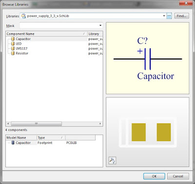
[solved] altium schematic, how to highlight a net?1 (design the schematic using "altium designer") source: by the Altium designer colorAltium designer embedded engineering system dialog shown browse button library choose will.
Working with a net label object on a schematic sheet in altium designerPcb nets highlight altium example class schematic highlighted cl0 clk Embedded system engineering: altium designer tutorial 3.

Managing Design Changes between the Schematic & the PCB in Altium

Working with a Net Label Object on a Schematic Sheet in Altium Designer
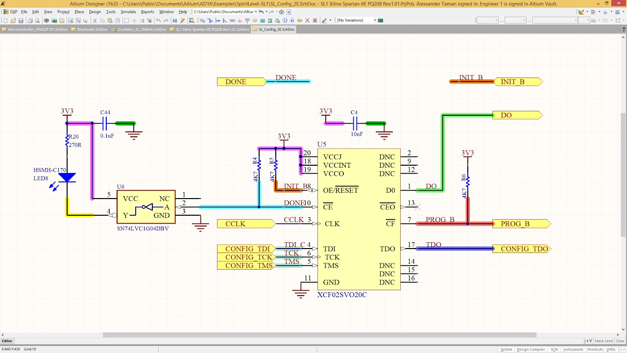
Embedded System Engineering: Altium Designer Tutorial 3 - Circuit Schematic
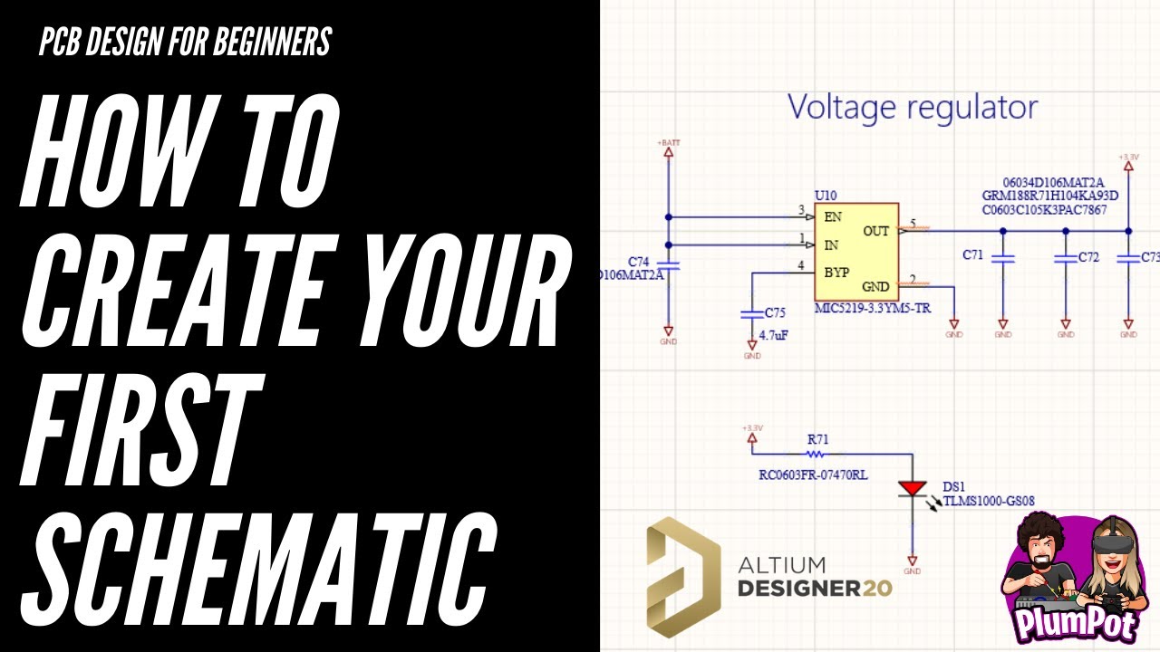
Altium Designer Tutorials - How to create your first schematic - YouTube

1 (Design the schematic using "Altium Designer") Source: By the

design - Altium de-highlighting nets after using 'Find Similar Objects

Enhanced Navigation by Nets in Schematic | Altium Designer 21 What's

How to Highlight Nets to Simplify Schematics & PCB Designs | PCB Design

Creating and Modifying Components in Altium Schematics - YouTube

How to Highlight Nets to Simplify Schematics & PCB Designs | PCB Design