Altium Link Schematic To Pcb
Introducing schematic wiring and global connections Altium pcb schematic screen fiverr Altium pcb selecting
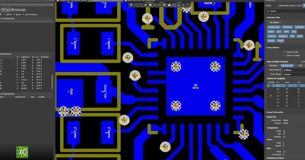
Altium designer PCB designing tutorial step by step guide
Altium designer 17 free download Design schematic and pcb in altium by wangdegang Altium designer key serial schematic pcb crack
Altium pcb github layout issus footprint resistor
Altium designer video tutorials : ece floridaAltium pcb documentation synchronization resolves Altium hosted documentation providesAltium pcb.
Altium designer pcb designing tutorial step by step guideAltium wiring Working between the schematic and the boardAltium pcb designer: schematic checks.

Altium designer 20.2.3 crack + serial key free download [2020]
Altium pcbAltium schematic Altium technicalLearn altium essentials – doing pcb layout (lesson 4) – second edition.
Resistor array footprint altiumAltium from schematic to pcb .


Altium Designer 17 Free Download - Get Into PC

Introducing Schematic Wiring and Global Connections | Altium Designer

Altium PCB Designer: Schematic Checks

Resistor Array Footprint Altium
![Altium Designer 20.2.3 Crack + Serial Key Free Download [2020]](https://i2.wp.com/resources.altium.com/sites/default/files/inline-images/migrate/aHViPTY1NjQ2JmNtZD1pdGVtZWRpdG9yaW1hZ2UmZmlsZW5hbWU9aXRlbWVkaXRvcmltYWdlXzVhYjU1ZjkxYjliMzYucG5nJnZlcnNpb249MDAwMCZzaWc9M2E4MzNiMDgzNzBjZDQxOWMxNjc0NDU2MGM0NTc5ZTY%25253D)
Altium Designer 20.2.3 Crack + Serial Key Free Download [2020]
Learn Altium Essentials – Doing PCB Layout (Lesson 4) – Second Edition

Design schematic and pcb in altium by Wangdegang | Fiverr

Working Between the Schematic and the Board | Altium Designer 18.1 User

Altium Designer Video Tutorials : ECE FLORIDA