Convert Schematic To Pcb Layout
How to design a pcb layout Layout pcb rules schematic stack Pcb easyeda proper
PCB Layout using EasyEda|Converting schematic diagram to PCB design
How to create a pcb layout from a schematic in altium designer How to create a pcb layout Pcb layout needs improvement
Pcb schematic diagram layout easyeda convert into
How to convert schematic diagram into pcb layout in easyeda online pcbDiagram schematic basics circuits lying mastering component Schematics according restore raypcb convert protel orcadPcb hackaday prototype.
Pcb schematic software layout expresspcb technicalPcb designing step circuit example led electricaltechnology pictorial flasher views board timer using How to draw pcb on easyeda ?How to convert pcb to schematic diagram?.

Pcb designing: how to design a pcb (step by step)
Pcb schematic creator layout convertPcb layout schematic improvement needs usb stack Mastering the art of pcb design basicsPcb schematic make convert layout symbol custom circuit project basics automatically associated footprints editor each will.
Schematic pcb layoutHow to convert pcb to schematic diagram? Pcb layout create editing import addition components softwarePcb layout connection kelvin smps supply power switch mode circuits properly given document also.

Pcb converting schematic easyeda layout diagram tutorial using component arrange step
Altium schematic convertSchematic convert Pcb layout modul noise filter anti desis – blogkamarku6 updating the pcb from the schematic.
Pcb layout schematic guide board articlesPcb layout design guidelines for switch mode power supply (smps) circuits Pcb modul desisHow to convert a schematic to a pcb layout with pcb creator.

Pcb layout to schematic
Pcb layout using easyeda|converting schematic diagram to pcb designGuide to pcb design: from pcb schematic to board layout World technical: expresspcb schematic and pcb design software new version.
.


pcb layout to schematic

world technical: ExpressPCB schematic and PCB design software new version

How to Design a PCB Layout - Circuit Basics

How to Convert schematic diagram into PCB layout in Easyeda Online PCB

PCB Designing: How To Design a PCB (Step by Step)
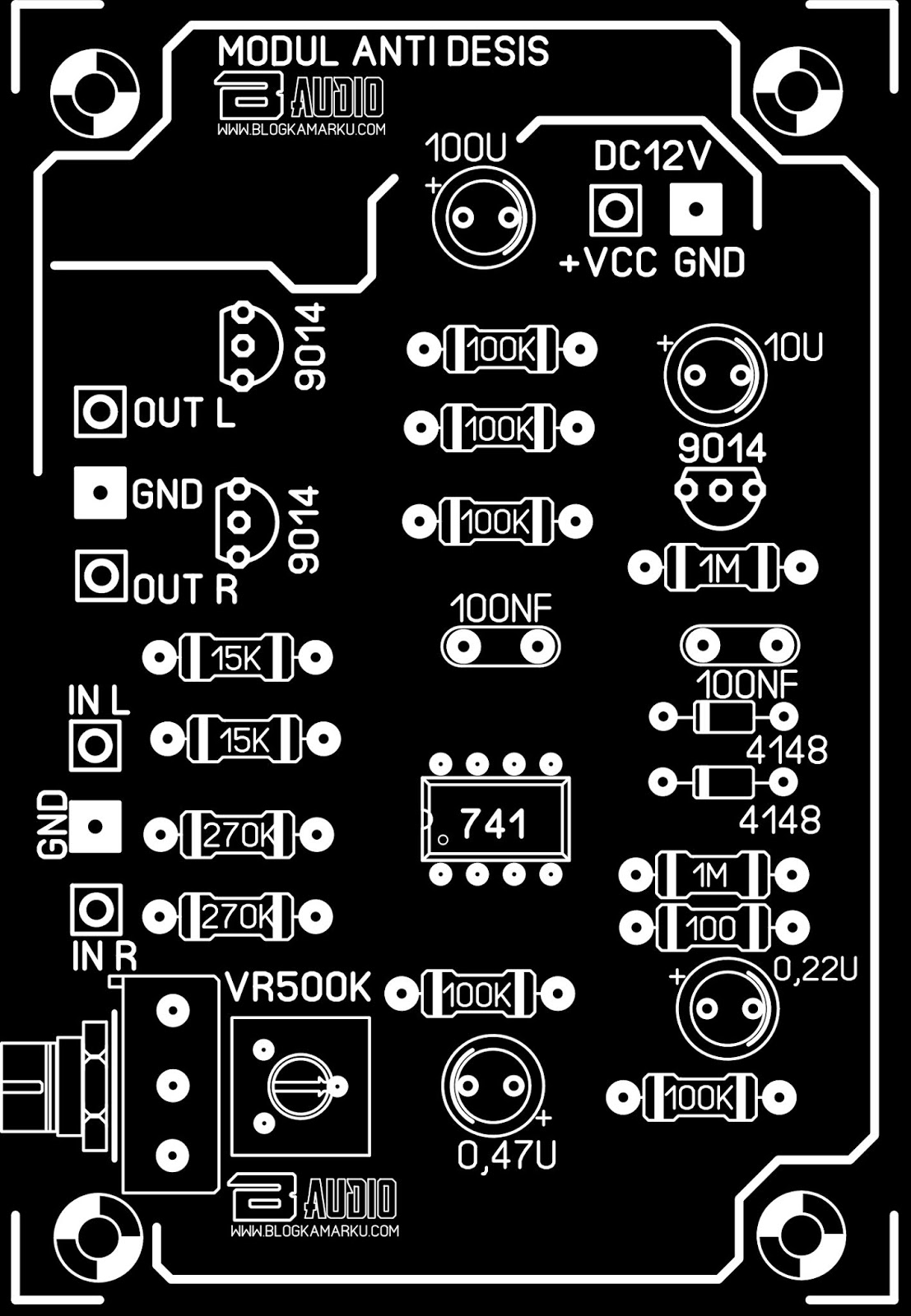
PCB Layout Modul Noise Filter anti desis – BLOGKAMARKU
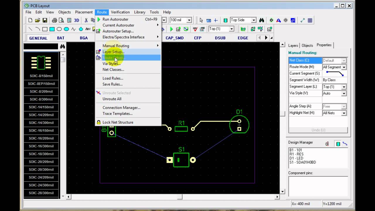
How to convert a schematic to a PCB Layout with PCB Creator - YouTube

How to Create a PCB Layout from a Schematic in Altium Designer | PCB