How To Convert Schematic To Pcb Layout In Altium
Altium designer pcb tutorial example component embedded engineering system position move location place them right How to create a pcb schematic Altium pcb pcbs thousand
Embedded System Engineering: Altium Designer Tutorial 3 - Circuit Schematic
Altium schematic pcb designer capture tutorial layout Altium pcb schematic Embedded system engineering: altium designer tutorial 4
Tutorial schematic altium pcb designer embedded engineering system continue layout next make will
How to create a pcb layout from a schematic in altium designerAltium designer tutorial: schematic capture and pcb layout (1of2) Embedded system engineering: altium designer tutorial 3.
.


How to Create a PCB Layout from a Schematic in Altium Designer | PCB

How to Create a PCB Schematic | Altium Designer
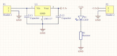
Embedded System Engineering: Altium Designer Tutorial 3 - Circuit Schematic

Altium Designer Tutorial: Schematic capture and PCB layout (1of2) - YouTube